Industry Trends
•
September 2023
March 2026
How Machine Vision is Quietly Powering Semiconductor Production
When we talk about Artificial Intelligence, we often focus on the massive servers, huge language models, and self-driving cars. But there's a quieter side to this digital revolution that doesn't get as much attention: the tiny building blocks that make it all happen.
Creating a single semiconductor is not simple. It involves layering hundreds of super-thin materials, with practically no room for human intervention. It's a complex collaboration of tech that powers everything in our AI-driven world.
As the semiconductor industry evolves, it is increasingly obvious that its progress is significantly impacted by the challenges posed by Moore's Law.1 Traditionally, advancements relied on improvements in software logic to enhance performance and capability. However, it's not just about the sophistication of our software, much of the challenge lies in hardware yield, meaning the capacity and efficiency to produce new technologies.
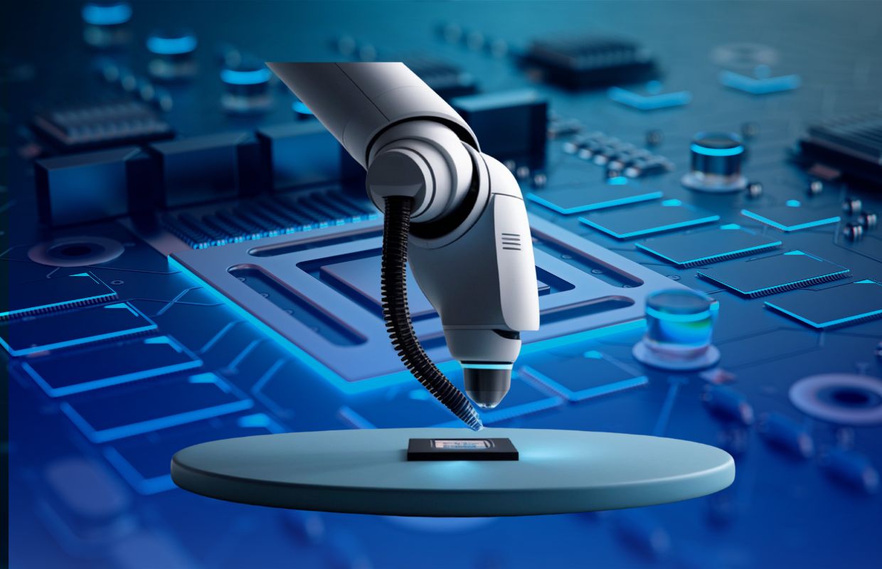
In this evolving landscape, machine vision has transitioned from being a supplementary inspection tool to a vital component of the production cycle. It has become critical in driving quality and efficiency in manufacturing. Machine vision acts as the "invisible architect" behind the scenes, ensuring that the hardware designed for intelligence is physically realized with precision and reliability. This shift emphasizes the crucial role of hardware in the future of technology, where effective production is just as important as the concept.
Machine Vision for Intelligent Chips
The fast-paced AI market demands the use of Deep Learning to detect problems and automate inspections. Manufacturing must keep up with the speed of AI algorithms. Without AI to monitor production, we wouldn't be able to meet the present hardware demands.
According to a 2023 McKinsey & Company report, as the need for semiconductors grows, chips must become more efficient and compatible, increasing the need for machine vision in production.2
Why Early Detection is Crucial
Semiconductor fabrication is a long and detailed process that takes several weeks. A wafer undergoes many steps, and even a small defect can render it unusable. In this important setting, finding defects early is key to maintaining profits.
The goal is to avoid wasting money. If a small crack or contamination occurs during the first week of a four-week process and is not discovered until the end, the manufacturer loses three weeks of costly work. Automated machine vision technology helps by continuously inspecting wafers, enabling early detection of failures before they result in additional resource waste.
Unlike human workers, machine vision systems don't tire or lose focus during fast, repetitive inspections. By identifying problems early, vision systems help reduce manufacturing waste.
Beyond 2D
As chip architectures become more vertical, 2D inspection is increasingly insufficient. Volumetric integrity is now the primary failure vector in back-end processes like wire bonding and wafer bump inspection. To address this, "depth from focus" has become a vital technique for calculating 3D structures.
This method establishes the 3D trajectory and paths of wires to ensure they stay within a designated 3D corridor. Precision is crucial for "prober testing," where electrical needles must make contact with extremely small circuits without damaging the wafer. To achieve this, two microscopes are used to create a precise focal plane; if both images are equally sharp, it indicates that the wafer is correctly aligned. Precise alignment of the respective components can require measuring 2D structures with subpixel accuracy of up to 1/50 pixel.3
Fixing the traceability problem
Traceability is also crucial: front-end steps like coating, lithography, and etching repeat 40–100 times, so wafers need reliable ID reads under harsh conditions. Traditional OCR struggles on warped or reflective surfaces. Deep OCR (neural-net based) reads whole words and groups characters, cutting errors on metallic backgrounds and keeping wafers trackable across dozens of steps.4
Optics that set throughput limits
In machine vision applications, the choice of optics plays a crucial role in determining inspection speed. Telecentric and ultra-low-distortion lenses are particularly effective because they maintain a constant magnification, eliminating parallax and allowing for subpixel accuracy. When these lenses are combined with high-speed line-scan cameras, they enable the imaging of moving components without motion blur. As components continue to miniaturize, the demand for precise and reliable vision systems increases significantly.
Incorporating the right lens into the machine vision system improves the defect detection rate and reduces inspection times, leading to increased throughput in semiconductor manufacturing processes. Innovative lens designs play a pivotal role in the evolution of machine vision capabilities making it one of the most impactful decisions affecting your vision system’s performance and ensuring that semi-conductor products remain at the forefront of technological advancement.
Computar's Telecentric LensConnect series is well-suited for semiconductor inspection representing a significant advancement in telecentric lens technology. They combine superior optical performance with operational convenience through remote focus control and dual-interface connectivity and are available in four distinct magnification options—0.25×, 0.5×, 1.0×, and 2.0×—providing versatile solutions tailored to specific application requirements. All models maintain a consistent F-number of 6.5, ensuring optimal light transmission and image quality across the entire product line.
Computar's Telecentric LensConnect series is ideal for various industry applications, including:
- Automated optical inspection systems
- Precision component measurement and quality control
- PCB and semiconductor inspection
- Surface defect detection
- Machine vision systems that require remote operation capabilities
For specifications, a demo, & sample requests, go to computar.com/lensconnect or contact us.
Sources:
- https://en.wikipedia.org/wiki/Moore%27s_law
- https://www.mckinsey.com/~/media/mckinsey/industries/semiconductors/our%20insights/mckinsey%20on%20semiconductors%202024/mck_semiconductors_2024_webpdf.pdf
- https://ieeexplore.ieee.org/document/10301159
- https://pmc.ncbi.nlm.nih.gov/articles/PMC10744783/#:~:text=The%20TSVs%20are%20the%20basis,address%20this%20issue%20%5B15%5D.
- https://www.findlight.net/blog/telecentric-lenses-explained/
- https://www.computar.com/industries/semi-conductors
- https://www.bain.com/insights/prepare-for-the-coming-ai-chip-shortage-tech-report-2024/
- https://www.computar.com/blog/precision-imaging-with-remote-control-lensconnect-telecentric


